General Description
The RT9471D is a highly-integrated 3A switch mode battery charge management and system power path management device for single cell Li-Ion and Li-polymer battery. The low impedance power path optimizes switch-mode operation efficiency, reduces battery charging time and extends battery life during discharging phase. The I2C serial interface with charging and system settings makes the device a truly flexible solution.
Performance Sepcification Summary
Summary of the RT9471D Evaluation Board performance specificiaiton is provided in Table 1. The ambient temperature is 25°C.
Table 1. RT9471D Evaluation Board Performance Specification Summary
|
Specification
|
Test Conditions
|
Min
|
Typ
|
Max
|
Unit
|
|
Input Voltage Range, VBUS
|
|
3.9
|
--
|
13.5
|
V
|
|
Maximum Input Current, IBUS
|
|
0
|
--
|
3.2
|
A
|
|
Maximum Input Current, IBUS
|
VBUS ≥ 12V
|
--
|
--
|
2
|
A
|
|
Maximum Output Current, ISYS
|
|
--
|
--
|
3.2
|
A
|
|
Maximum Battery Voltage, VBAT
|
|
--
|
--
|
4.7
|
V
|
|
Maximum Charge Current, IBAT
|
|
--
|
--
|
3.15
|
A
|
|
Maximum Discharge Current, IBAT
|
|
--
|
--
|
6
|
A
|
Power-up Procedure
Suggestion Required Equipments
- RT9471D Evaluation Board
- DC power supply x 2, one for VBAT, one for VBUS
- Electronic load
- Oscilloscope
Quick Start Procedures
The Evaluation Board is fully assembled and tested. Follow the steps below to verify board operation. Do not turn on supplies until all connections are made.
Proper measurement equipment setup and follow the procedure below.
1. Set power source equal 3.8V/5A then connect to BAT and GND of EVB.
2. Use E-Load connect to power source and enable CC loading from power source.
3. The AP connect to SCL, SDA and GND of EVB
4. Check I2C can work normally by connecting to slave address (0x53).
5. Set VBUS = 5V/3A and connect to VBUS and GND of EVB.
6. Check have charging current to VBAT.
7. Check 0x0F[3:0] shows ‘0100’ (Fast-charge)
8. Start the test by changing register setting which you want.
Detailed Description of Hardware
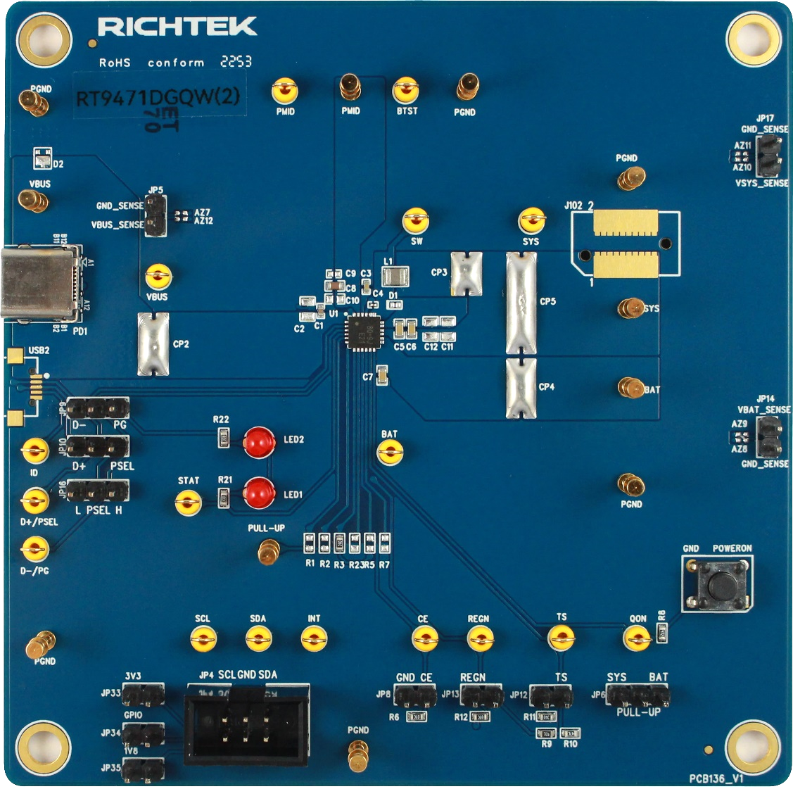
Headers Description and Placement
Carefully inspect all the components used in the EVB according to the following Bill of Materials table, and then make sure all the components are undamaged and correctly installed. If there is any missing or damaged component, which may occur during transportation, please contact our distributors or e-mail us at evb_service@richtek.com.
Test Points
The EVB is provided with the test points and pin names listed in the table below.
|
Test Point/
Pin Name
|
Function
|
|
VBUS
|
Input voltage.
|
|
SYS
|
System voltage.
|
|
BAT
|
Battery voltage.
|
|
SW
|
Switching node.
|
|
REGN
|
Internal LDO.
|
|
PMID
|
PMID from VBUS.
|
|
BTST
|
Boost strap pin.
|
|
INT
|
Interupt pin.
|
|
SDA
|
I2C SDA.
|
|
SCL
|
I2C SCL.
|
|
/QON
|
Power key.
|
|
VAC
|
Input sense.
|
|
/CE
|
Charger enable or disable.
|
|
D+
|
Positive of USB data line.
|
|
D-
|
Negative of USB data line.
|
|
TS
|
Temperature sense voltage.
|
Bill of Materials
|
Reference
|
Count
|
Part Number
|
Description
|
Package
|
Vendor
|
|
C1
|
1
|
GRM155R61E105KA12
|
1µF/25V/X5R/0402
|
0402
|
Murata
|
|
C3
|
1
|
GRM155R60J475ME47
|
4.7µF/6.3V/X5R/0402
|
0402
|
Murata
|
|
C4
|
1
|
GRM033R61C473KE84
|
47nF/16V/X5R/0201
|
0201
|
Murata
|
|
C5, C6, C7
|
2
|
GRM185R60J106ME15
|
10µF/6.3V/X5R/0603
|
0603
|
Murata
|
|
C10
|
1
|
GRM188R61E106MA73
|
10µF/25V/X5R/0603
|
0603
|
Murata
|
|
J102
|
1
|
HSEC8-110-01-S-DV-A-TR
|
CONN EDGE DUAL FMALE 20POS 0.8mm
|
12.6x7.98mm
|
SAMTEC
|
|
L1
|
1
|
CIGT252010EH1R0MNE
|
1µH
|
L-2-5x2-0
|
Samsung
|
|
LED1, LED2
|
2
|
LNL-302RD000A1
|
LED_RED-DIP
|
LED-3-85MMDIP
|
LighTop
|
|
PD1
|
1
|
121U-3CST-09CR
|
USB TYPE-C 3.1
|
9.87x9.75mm
|
JEM
|
|
POWER
ON
|
1
|
HTS6601H
|
SW-TACT-SWITCH
|
TACT-BTN
|
High-Tronics
|
|
R3, R6,
R11, R12
|
4
|
WR06X1002FTL
|
10k/0603
|
0603
|
WALSIN
|
|
R8
|
1
|
WR06X4701FTL
|
4.7k/0603
|
0603
|
WALSIN
|
|
R9
|
1
|
WR06X5231FTL
|
5.23k/0603
|
0603
|
WALSIN
|
|
R10
|
1
|
WR06X3012FTL
|
30.1k/0603
|
0603
|
WALSIN
|
|
R21, R22
|
2
|
WR06X2001FTL
|
2k/0603
|
0603
|
WALSIN
|
|
U1
|
1
|
RT9471DGQW(2)
|
RT9471DGQW(2)
|
WQFN-24L 4x4
|
RichTek
|
|
USB2
|
1
|
UMMBF-051MGCB2-CF1066
|
MICRO USB AB TYPE, SMT
|
7.4x5.63mm
|
Cherng Weei
|
Typical Applications
EVB Schematic Diagram
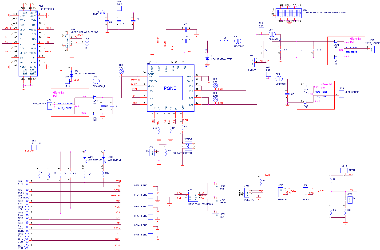
1. The capacitance values of the input and output capacitors will influence the input and output voltage ripple and stability.
2. MLCC capacitors have degrading capacitance at DC bias voltage, and especially smaller size MLCC capacitors will have much lower capacitance.
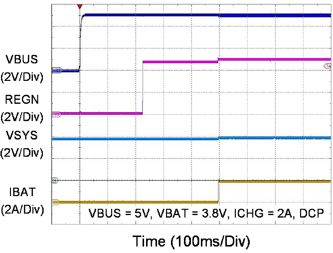
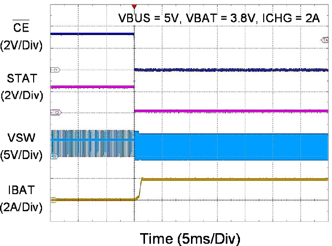
Measure Result
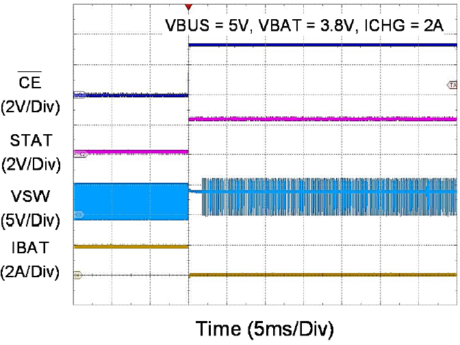
|
Power –Up with VBUS Plug In
|
Charge Enable
|
|
|
|
|
Charge Disable
|
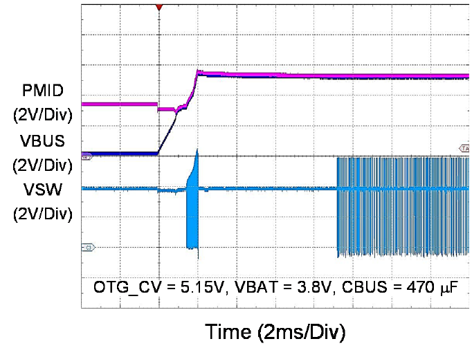
Boost Start-Up
|
|
|
|
|
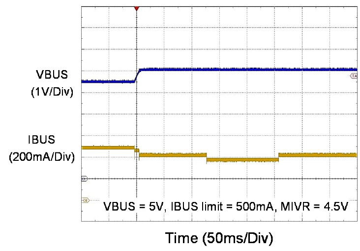
AICC Enable
|
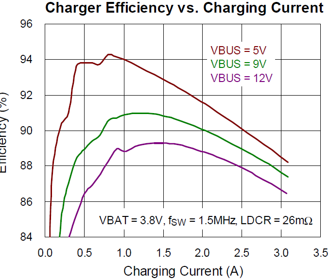
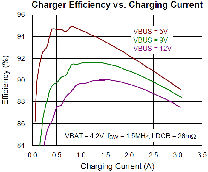
Charger Efficiency, VBAT = 3.8V
|
|
|
|
|
Charger Efficiency, VBAT = 4.2V
|
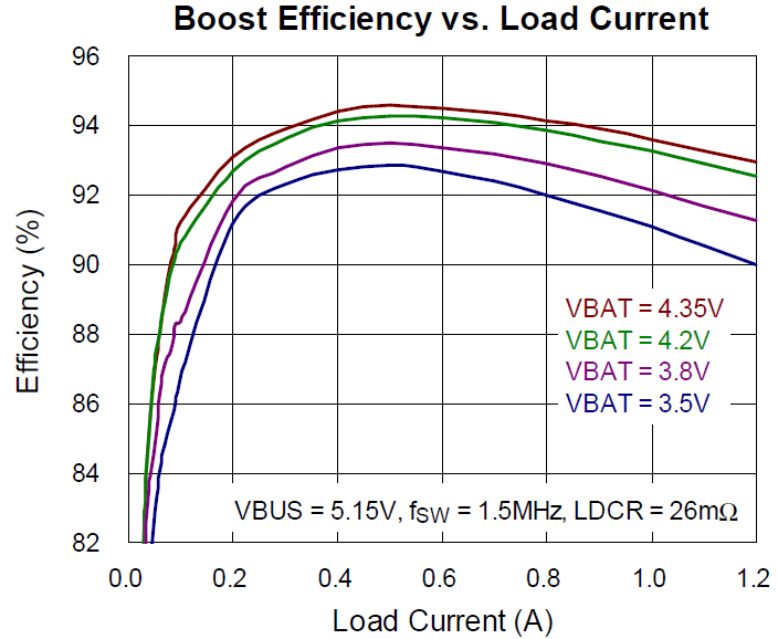
Boost Efficiency
|
|
|
|
Evaluation Board Layout
Figure 1 to Figure 4 are RT9471D Evaluation Board layout.
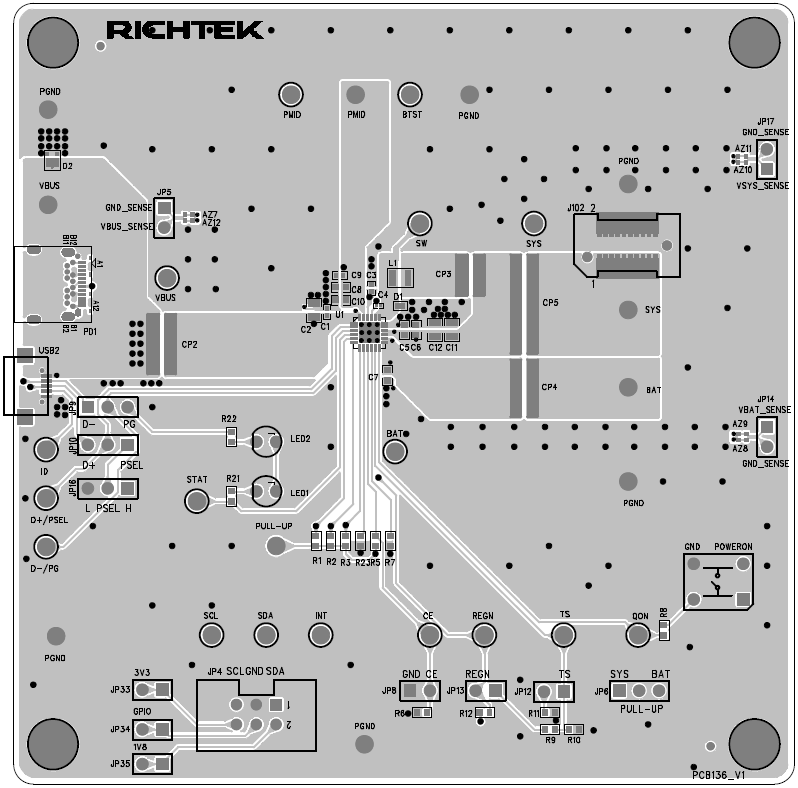
Figure 1. Top View (1st layer)
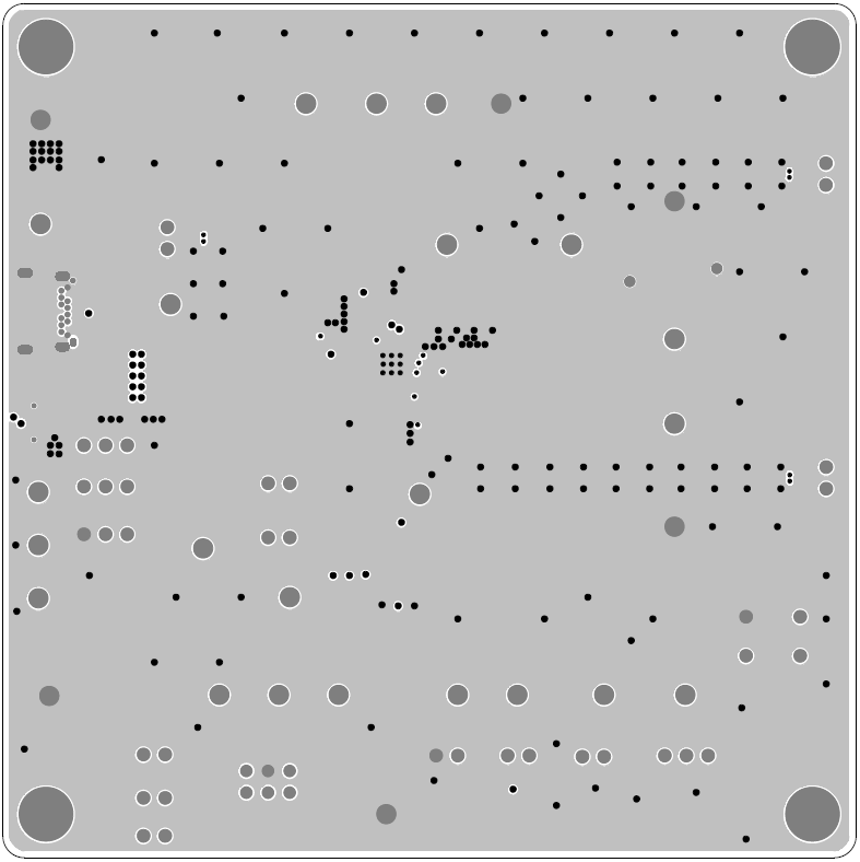
Figure 2. PCB Layout—Inner Side (2nd Layer)
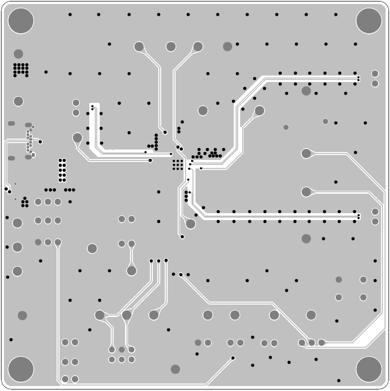
Figure 3. PCB Layout—Inner Side (3rd Layer)
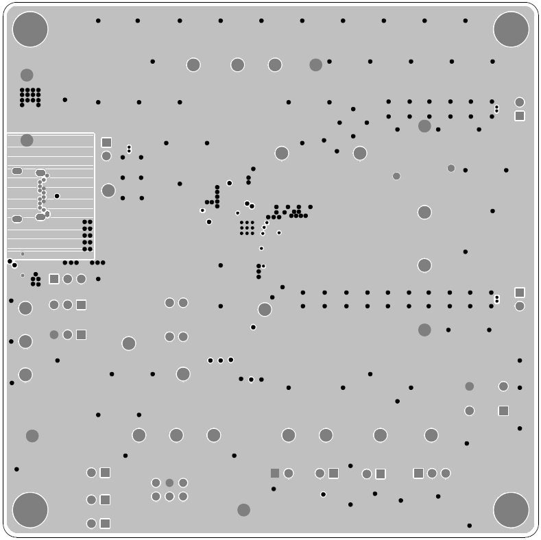
Figure 4. Bottom View (4th Layer)